【电机控制】FOC单电阻电流采样配置
文章目录
- 前言
- 1 基本原理
- 2 核心功能函数
- 2.1 基本设置
- 2.2 获取CCR排序
- 2.2 判断PWM是否需要偏移以及需要偏移多少,并确定ADC采样点,判断采样电流的相以及方向
- 2.3 结合具体MCU型号的TIM以及DMA配置
- 总结
前言
本文记录笔者在学习单电阻采样代码实现过程中的总结和思考。
1 基本原理
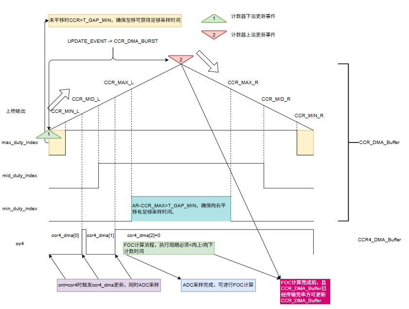
笔者默认本文读者对单电阻采样的原理层面已经有了基本的理解,因此仅提供如下采样时序图以及编程中一些需要重点考虑的事项。
这里省略采样前的各相占空比需求和CCR计算。
2 核心功能函数
2.1 基本设置
最小采样间隔时间以及其中包含的死区、开通时间、稳定时间等需要实验测定。
2.2 获取CCR排序
前面已经获取duty或ccr值,两两比较后分别赋值给max_duty_index, mid_duty_index, min_duty_index。比较简单,如下是代码段参考
#define u 0
#define v 1
#define w 2void FOC_InvClark_Tr(FOC_t *foc)
{int16_t com;foc->pCtl->Vph.s_volt[u] = foc->pCtl->Vab.va;foc->pCtl->Vph.s_volt[v] = -foc->pCtl->Vab.va / 2 + Q_Mpy(foc->pCtl->Vab.vb, SQRT3DIV2_Q);foc->pCtl->Vph.s_volt[w] = -foc->pCtl->Vab.va / 2 - Q_Mpy(foc->pCtl->Vab.vb, SQRT3DIV2_Q);if (foc->pCtl->Vph.s_volt[u] >= foc->pCtl->Vph.s_volt[v]){if (foc->pCtl->Vph.s_volt[v] >= foc->pCtl->Vph.s_volt[w]){foc->pCtl->Svpwm.max_duty_phase = u;foc->pCtl->Svpwm.mid_duty_phase = v;foc->pCtl->Svpwm.min_duty_phase = w;}else{if (foc->pCtl->Vph.s_volt[u] >= foc->pCtl->Vph.s_volt[w]){foc->pCtl->Svpwm.max_duty_phase = u;foc->pCtl->Svpwm.mid_duty_phase = w;foc->pCtl->Svpwm.min_duty_phase = v;}else{foc->pCtl->Svpwm.max_duty_phase = w;foc->pCtl->Svpwm.mid_duty_phase = u;foc->pCtl->Svpwm.min_duty_phase = v;}}}else{if (foc->pCtl->Vph.s_volt[u] >= foc->pCtl->Vph.s_volt[w]){foc->pCtl->Svpwm.max_duty_phase = v;foc->pCtl->Svpwm.mid_duty_phase = u;foc->pCtl->Svpwm.min_duty_phase = w;}else{if (foc->pCtl->Vph.s_volt[v] >= foc->pCtl->Vph.s_volt[w]){foc->pCtl->Svpwm.max_duty_phase = v;foc->pCtl->Svpwm.mid_duty_phase = w;foc->pCtl->Svpwm.min_duty_phase = u;}else{foc->pCtl->Svpwm.max_duty_phase = w;foc->pCtl->Svpwm.mid_duty_phase = v;foc->pCtl->Svpwm.min_duty_phase = u;}}}/* Insert 3rd harmonic component to generate saddle wave. */com = (foc->pCtl->Vph.s_volt[foc->pCtl->Svpwm.max_duty_phase] >> 1) + ((foc->pCtl->Vph.s_volt[foc->pCtl->Svpwm.min_duty_phase] + 1) >> 1);/* Circle limit assure duty cycle is not over 100% or less than 0%. */foc->pCtl->Vph.u_volt[u] = (uint16_t)((int32_t)foc->pCtl->Vph.s_volt[u] + (foc->pCtl->vdcPu >> 1) - com);foc->pCtl->Vph.u_volt[v] = (uint16_t)((int32_t)foc->pCtl->Vph.s_volt[v] + (foc->pCtl->vdcPu >> 1) - com);foc->pCtl->Vph.u_volt[w] = (uint16_t)((int32_t)foc->pCtl->Vph.s_volt[w] + (foc->pCtl->vdcPu >> 1) - com);
}
2.2 判断PWM是否需要偏移以及需要偏移多少,并确定ADC采样点,判断采样电流的相以及方向
代码如下(示例):
void FOC_Generate_Svpwm(FOC_t *foc)
{foc->pCtl->Svpwm.duty[u] = (uint32_t)foc->pCtl->Vph.u_volt[u] << 16 / foc->pCtl->vdcPu;foc->pCtl->Svpwm.duty[v] = (uint32_t)foc->pCtl->Vph.u_volt[v] << 16 / foc->pCtl->vdcPu;foc->pCtl->Svpwm.duty[w] = (uint32_t)foc->pCtl->Vph.u_volt[w] << 16 / foc->pCtl->vdcPu;foc->pCtl->Svpwm.ccr[u] = PWM_TIME_PERIOD - (uint32_t)foc->pCtl->Vph.u_volt[u] * PWM_TIME_PERIOD / foc->pCtl->vdcPu;foc->pCtl->Svpwm.ccr[v] = PWM_TIME_PERIOD - (uint32_t)foc->pCtl->Vph.u_volt[v] * PWM_TIME_PERIOD / foc->pCtl->vdcPu;foc->pCtl->Svpwm.ccr[w] = PWM_TIME_PERIOD - (uint32_t)foc->pCtl->Vph.u_volt[w] * PWM_TIME_PERIOD / foc->pCtl->vdcPu;// foc->pCtl->Svpwm.ccr[u] = (uint16_t)Math_Sat(ccu, T_MAX, T_MIN);// foc->pCtl->Svpwm.ccr[v] = (uint16_t)Math_Sat(ccv, T_MAX, T_MIN);// foc->pCtl->Svpwm.ccr[w] = (uint16_t)Math_Sat(ccw, T_MAX, T_MIN);#ifdef SINGLE_SHUNT_SAMPLEint8_t max_ccr_index, mid_ccr_index, min_ccr_index;max_ccr_index = foc->pCtl->Svpwm.min_duty_phase;mid_ccr_index = foc->pCtl->Svpwm.mid_duty_phase;min_ccr_index = foc->pCtl->Svpwm.max_duty_phase;/*  * __为低电平* ##为高电平* !为采样点* 情况1: 三相占空比间隔时间足够采样;* max ___#!##########___* mid _____#!######_____       ===>>>          NO SHIFT* min _______####_______* 情况2: 低调制比情况下,两两之间采样时间均不足* max ______######______                       max ____#!####________* mid ______######______       ===>>>          mid ______#!####______       以最中值为基准,max向左边平移,min向右边平移* min ______######______                       min ________######____       * 情况3: 换相时,两相间隔时间不足采样;细分为高高低,高低低两种情况,高高低的* max __##############__                       max _#!############___       * mid __##############__       ===>>>          mid ___#!############_       以中值为基准,max向左边平移* min _______####_______                       min _______####_______* max _################_                       max _#!##############_* mid _______####_______       ===>>>          mid _______#!##_______       以中值为基准,min向右边平移* min _______####_______                       min _________####_____       *! 为确保采样时间足够,并通过单次平移实现足够采样时间,CCR_MAX < PERIOD - T_GAP_MIN, CCR_MIN > T_GAP_MIN*/int16_t d_max_mid, d_mid_min;int16_t ccr_max_shift, ccr_min_shift;d_max_mid = foc->pCtl->Svpwm.ccr[max_ccr_index] - foc->pCtl->Svpwm.ccr[mid_ccr_index];d_mid_min = foc->pCtl->Svpwm.ccr[mid_ccr_index] - foc->pCtl->Svpwm.ccr[min_ccr_index];if (foc->pCtl->Svpwm.ccr[mid_ccr_index] - foc->pCtl->Svpwm.ccr[min_ccr_index] >= T_GAP_MIN){//ccr min index phase sample time OK. Current direction is positive.}else{ccr_min_shift = T_GAP_MIN - d_mid_min;if (foc->pCtl->Svpwm.ccr[min_ccr_index] > ccr_min_shift){// Shift action must confirm that right ccr value is greater than 0foc->pCtl->Svpwm.ccr_dma_buffer_latch[min_ccr_index] = foc->pCtl->Svpwm.ccr[min_ccr_index] - ccr_min_shift;foc->pCtl->Svpwm.ccr_dma_buffer_latch[min_ccr_index + 3] = foc->pCtl->Svpwm.ccr[min_ccr_index] + ccr_min_shift;foc->pCtl->Svpwm.adc_signal[0] = 1;}else{/* Shift space is not enough. Est current inherit from last cycle. Skip flag required. */foc->pCtl->Svpwm.ccr_dma_buffer_latch[min_ccr_index] = foc->pCtl->Svpwm.ccr[min_ccr_index];foc->pCtl->Svpwm.ccr_dma_buffer_latch[min_ccr_index + 3] = foc->pCtl->Svpwm.ccr[min_ccr_index];foc->pCtl->Svpwm.adc_signal[0] = 0;}}if (foc->pCtl->Svpwm.ccr[max_ccr_index] - foc->pCtl->Svpwm.ccr[mid_ccr_index] >= T_GAP_MIN){//ccr max index phase sample time OK. Current direction is negative.}else{ccr_max_shift = T_GAP_MIN - d_max_mid;// Shift action must confirm that left ccr value is less than ARif (foc->pCtl->Svpwm.ccr[max_ccr_index] + ccr_max_shift < PWM_TIME_PERIOD){foc->pCtl->Svpwm.ccr_dma_buffer_latch[max_ccr_index] = foc->pCtl->Svpwm.ccr[max_ccr_index] + ccr_max_shift;foc->pCtl->Svpwm.ccr_dma_buffer_latch[max_ccr_index + 3] = foc->pCtl->Svpwm.ccr[max_ccr_index] - ccr_max_shift;foc->pCtl->Svpwm.adc_signal[1] = -1;}else{/* Shift space is not enough. Est current inherit from last cycle. Skip flag required. */foc->pCtl->Svpwm.ccr_dma_buffer_latch[max_ccr_index] = foc->pCtl->Svpwm.ccr[max_ccr_index];foc->pCtl->Svpwm.ccr_dma_buffer_latch[max_ccr_index + 3] = foc->pCtl->Svpwm.ccr[max_ccr_index];foc->pCtl->Svpwm.adc_signal[1] = 0;}}foc->pCtl->Svpwm.ccr_dma_buffer_latch[mid_ccr_index] = foc->pCtl->Svpwm.ccr[mid_ccr_index];foc->pCtl->Svpwm.ccr_dma_buffer_latch[mid_ccr_index + 3] = foc->pCtl->Svpwm.ccr[mid_ccr_index];/* Set CCR4 to the very first sampling pointwhen CNT matches CCR4 value (first sampling point), it raises CH4 signal:- it triggers the first ADC injected conversion- it triggers a DMA transfer to load CCR4 with the second sampling valuewhich lowers CH4 signal.when CNT matches CCR4 value (second sampling point value) it raises CH4 signal- it triggers the second ADC injected conversion- it triggers a DMA to transfer to load 0 into CCR4 register which makes CH4stay high until next PWM cyclewhen CNT matches CCR4 value (0 i.e start of a new PWM cycle) it lowers CH4 signal- it triggers a DMA to transfer to load CCR4 with the first sampling point value */foc->pCtl->Svpwm.ccr_adc[0] = foc->pCtl->Svpwm.ccr_dma_buffer_latch[min_ccr_index] + T_RISE;foc->pCtl->Svpwm.ccr_adc[1] = foc->pCtl->Svpwm.ccr_dma_buffer_latch[mid_ccr_index] + T_RISE;foc->pCtl->Svpwm.ccr_adc[2] = 0;foc->pCtl->Svpwm.adc_index[0] = min_ccr_index;foc->pCtl->Svpwm.adc_index[1] = max_ccr_index;foc->pCtl->Svpwm.adc_signal[0] = 1;foc->pCtl->Svpwm.adc_signal[1] = -1;#endif
}
2.3 结合具体MCU型号的TIM以及DMA配置
本文以国民N32G435的配置为例:
总结
本文借鉴了ST MCSDK单电阻采样的写法,但也有诸多配置和策略上的不同,代码是笔者手敲的,仅供参考,欢迎指正。
注:笔者并没有采用常规的六分区写法,而是采用了三次谐波插入法做变换计算生成马鞍波。